hankyoreh
Links to other country sites 다른 나라 사이트 링크
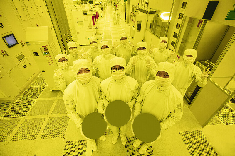
Samsung becomes first mass producer of 3nm chips, ahead of TSMC
On Thursday, Samsung Electronics became the first chip foundry in the world to begin mass production of semiconductors through a 3-nanometer process based on gate-all-around (GAA) technology.
Experts say the company has now established the technological foundation on which to outstrip Taiwan Semiconductor Manufacturing Co., or TSMC, the No. 1 foundry in the world. Others say it will take the South Korean semiconductor giant some time to achieve a yield rate high enough to secure significant clients like Qualcomm.
The 3-nanometer process is the most advanced semiconductor manufacturing process to date, allowing for the production of chips with a circuit width that is 0.00003 times as thick as a strand of human hair. The thinner the circuit width can be made, the easier it is to improve the performance of semiconductors through miniaturization via high integration as well as through the reduction of power usage.
According to Omdia, a market research company, Samsung Electronics made 20 trillion won in sales through its foundry business last year, which accounted for 7% of the company’s total sales figure of 280 trillion won that year.
Meanwhile, the company’s market share in the semiconductor industry is 16.3%, still significantly behind TSMC’s 49.5%.
Samsung Electronics became the first in the world to make use of GAA technology instead of the standard finFET technology. A key component of semiconductors, transistors are divided into two types: channel transistors, through which electricity flows, and gate transistors, which control the electric current. Unlike the three-dimensional structure of chips made with finFET technology, chips made with GAA technology have channel transistors that are shielded on all four sides — including the bottom — by gate transistors, allowing for even more minute control of the electric current.
“Compared to 5nm process, the first-generation 3nm process can reduce power consumption by up to 45%, improve performance by 23% and reduce area by 16%,” Samsung Electronics explained in a press release. The company continued, “The second-generation 3nm process is to reduce power consumption by up to 50%, improve performance by 30% and reduce area by 35%.”
Choi Si-young, president of Samsung Electronics’ Foundry Business Division, said, “We will continue active innovation in competitive technology development and build processes that help expedite achieving maturity of technology.”
Although Samsung Electronics has gotten a step ahead in terms of technological advancement, observers say it may take a while for the company to secure clients willing to consign it with semiconductor manufacturing. As the new process is in its first generation, its yield rate may not be high enough, and the company will have to reclaim large clients such as Qualcomm and Nvidia from TSMC.
After consigning Samsung Electronics to manufacture Snapdragon 8 Gen 1 application processors, which were used in mobile phones like the Galaxy S22, last year, Qualcomm gave its foundry order for the Snapdragon 8+ Gen 1 and Snapdragon 8 Gen 2 to TSMC.
Nvidia has also consistently tapped TSMC to supply its GPUs, demand for which is growing due to the popularization of artificial intelligence.
Korea Institute for Industrial Economics and Trade (KIET) researcher Kim Yang-paeng commented, “[Samsung Electronics] showcased its technological prowess by becoming the first to start the 3-nanometer process in the world, through which [it] will be able to improve the performance of [its] products.” He added, “Still, as [the process] is in its first generation and in a trial process, it will be difficult for [the company] to secure many clients, which is why it’s unclear if [introduction of the 3-nanometer process] will lead to profits.”
An analyst at a securities firm who spoke on the condition of anonymity said, “Even Samsung Electronics itself doesn’t have plans to manufacture a follow-up product to its own application processor Exynos, so there are really no clients that would use the recently unveiled 3-nanometer process.”
Reducing carbon emissions is another challenge faced by Samsung Electronics. A significant amount of greenhouse gases is used during the semiconductor manufacturing process, such as during the etching process, when substance layers are removed from wafers, and during the deposition process, when layers are created. Unused greenhouse gases are discharged into the atmosphere in significant amounts during these processes.
“The more advanced semiconductor manufacturing processes become, the more power they consume and the more greenhouse gasses they emit,” KIET researcher Nam Sang-wook said. “To achieve carbon neutrality, efforts are needed to figure out ways to increase the use of renewable energy and develop alternate gases that emit less carbon.”
Unlike TSMC and SK Hynix, Samsung Electronics did not join RE100, a global initiative of corporations committed to sourcing 100% of their electricity usage with renewable energy by 2050.
By Lee Jeong-hun, staff reporter
Please direct questions or comments to [english@hani.co.kr]

Editorial・opinion
![[Editorial] Yoon must halt procurement of SM-3 interceptor missiles](https://flexible.img.hani.co.kr/flexible/normal/500/300/imgdb/child/2024/0501/17145495551605_1717145495195344.jpg "[Editorial] Yoon must halt procurement of SM-3 interceptor missiles") [Editorial] Yoon must halt procurement of SM-3 interceptor missiles
[Editorial] Yoon must halt procurement of SM-3 interceptor missiles![[Guest essay] Maybe Korea’s rapid population decline is an opportunity, not a crisis](https://flexible.img.hani.co.kr/flexible/normal/500/300/imgdb/original/2024/0430/9417144634983596.jpg "[Guest essay] Maybe Korea’s rapid population decline is an opportunity, not a crisis") [Guest essay] Maybe Korea’s rapid population decline is an opportunity, not a crisis
[Guest essay] Maybe Korea’s rapid population decline is an opportunity, not a crisis- [Column] Can Yoon steer diplomacy with Russia, China back on track?
- [Column] Season 2 of special prosecutor probe may be coming to Korea soon
- [Column] Park Geun-hye déjà vu in Yoon Suk-yeol
- [Editorial] New weight of N. Korea’s nuclear threats makes dialogue all the more urgent
- [Guest essay] The real reason Korea’s new right wants to dub Rhee a founding father
- [Column] ‘Choson’: Is it time we start referring to N. Korea in its own terms?
- [Editorial] Japan’s rewriting of history with Korea has gone too far
- [Column] The president’s questionable capacity for dialogue
Most viewed articles
- 1Months and months of overdue wages are pushing migrant workers in Korea into debt
- 2Trump asks why US would defend Korea, hints at hiking Seoul’s defense cost burden
- 3At heart of West’s handwringing over Chinese ‘overcapacity,’ a battle to lead key future industries
- 4[Editorial] Yoon must halt procurement of SM-3 interceptor missiles
- 5Fruitless Yoon-Lee summit inflames partisan tensions in Korea
- 61 in 3 S. Korean security experts support nuclear armament, CSIS finds
- 7Dermatology, plastic surgery drove record medical tourism to Korea in 2023
- 8AI is catching up with humans at a ‘shocking’ rate
- 9First meeting between Yoon, Lee in 2 years ends without compromise or agreement
- 10Amnesty notes ‘erosion’ of freedom of expression in Korea in annual human rights report