hankyoreh
Links to other country sites 다른 나라 사이트 링크
Samsung’s new strategy swaps tech breakthroughs for a focus on customer service
During this year’s Samsung Foundry Forum, the Korean electronics maker has focused on customer service as its main strategy. This stands in contrast to past strategies of emphasizing technological prowess and setting itself apart from the competition.
Instead of trying to go head-to-head with Taiwan’s TSMC in terms of technical ability, Samsung has opted to take advantage of its position as a comprehensive semiconductor firm and offer a customer-friendly one-stop service. It remains to be seen whether Samsung will be able to distinguish itself among its three major competitors: Nvidia, TSMC and SK Hynix.
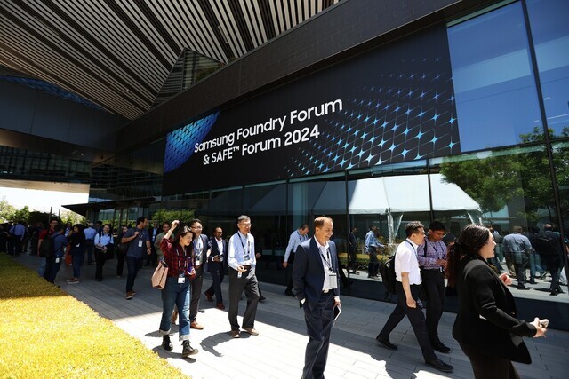
According to a press release by Samsung on Thursday, key fabless clients and partners attended the Samsung Foundry Forum and Samsung Advanced Foundry Ecosystem (SAFE) Forum in Silicon Valley on Wednesday under the theme “Empowering the AI Revolution.”
What’s notable is that Samsung did not attempt to present itself as a contender in the competition surrounding the ultra-fine processes that go into semiconductor manufacturing. At the forum, Samsung representatives merely reiterated previous statements regarding plans for 1.4 nanometer processes in 2027 to reach target technical and supply goals.
This past April, TSMC announced plans to introduce 1 nanometer processes by 2026, a full year ahead of the original announcements proclaiming 2027. Yet Samsung did not attempt to one-up its competitor at the forum. Last year, Samsung ramped up the narrative pressure against TSMC by announcing the industry’s first plans for processes less than 2 nanometers as well as a roadmap for 2 nm processes. This year, however, Samsung has changed gears.
Regarding ultra-fine processes, Samsung merely announced changes in the smaller details. Using backside power delivery network (BSPDN) technology, Samsung announced that its SF2Z process node will be ready for mass production in 2027. The BSPDN model places the power rails on the backside of the wafer containing the circuit, as opposed to the front. This minimizes the bottleneck effect that occurs during the transmission of electronic signals, thereby improving consumptive power and performance. TSMC has announced plans to introduce this model by 2026.
Instead of competing on the technical front, Samsung revised its strategy to pull from its experience and infrastructure as a comprehensive electronics and semiconductor firm, focusing on providing “one-stop AI solutions.” As a firm that operates its own foundry, manufactures its own memory technology, and offers cutting-edge packaging, Samsung claims it is positioned to offer a full-package customer experience that other firms, which are more specialized, cannot offer.
With the advent of AI technology, large amounts of data can be quickly relayed and processed, the convergence of system semiconductors with semiconductor memory is becoming increasingly important. Fabless firms have to outsource the foundry, memory and packaging processes. If the time they require to complete everything from development to production is 100, then Samsung claims that its vertically integrated manufacturing chains allows it to reduce that to 80.
Regarding this sudden shift in strategy, industry analysts point to the infeasibility of relying on technological superiority in the foundry industry. In 2022, Samsung beat TSMC to the punch in introducing 3 nm processes, but this did not result in any significant revenue advantages over its competitor. Rather, TSMC has actually increased its market share since then, widening the gap with Samsung. Industry insiders think that a reduction in transference numbers is holding Samsung back. The firm seems to have concluded that ultra-fine processes in semiconductor manufacturing are slowly reaching their limit.
“Retention numbers and profitability when it comes to cutting-edge semiconductors aren’t great, so Samsung has switched strategies. Rather than the cutting-edge market, it looks like they're shifting gears to the 5-10 nanometer processes,” said Kim Yang-paeng, a researcher at the Korea Institute for Industrial Economics and Trade.
But there are questions about whether Samsung’s new “one-stop service” strategy will work. Currently, Nvidia exercises an effective monopoly over the market for AI chips. Nvidia has already secured a trilateral manufacturing network that employs TSMC’s foundry and SK Hynix’s memory technology. A Samsung representative said, “It’s a strategy that considers various aspects of the fabless model.”
By Lee Jae-yeon, staff reporter
Please direct questions or comments to [english@hani.co.kr]

Editorial・opinion
![[Editorial] Exploiting foreign domestic workers won’t solve Korea’s birth rate problem](https://flexible.img.hani.co.kr/flexible/normal/500/300/imgdb/original/2024/0626/5517193887628759.jpg "[Editorial] Exploiting foreign domestic workers won’t solve Korea’s birth rate problem") [Editorial] Exploiting foreign domestic workers won’t solve Korea’s birth rate problem
[Editorial] Exploiting foreign domestic workers won’t solve Korea’s birth rate problem![[Column] Kim and Putin’s new world order](https://flexible.img.hani.co.kr/flexible/normal/500/300/imgdb/original/2024/0625/9617193034806503.jpg "[Column] Kim and Putin’s new world order") [Column] Kim and Putin’s new world order
[Column] Kim and Putin’s new world order- [Editorial] Workplace hazards can be prevented — why weren’t they this time?
- [Editorial] Seoul failed to use diplomacy with Moscow — now it’s resorting to threats
- [Column] Balloons, drones, wiretapping… Yongsan’s got it all!
- [Editorial] It’s time for us all to rethink our approach to North Korea
- [Column] Why empty gestures matter more than ever
- [Editorial] Seoul’s part in N. Korea, Russia upgrading ties to a ‘strategic partnership’
- [Column] The tragedy of Korea’s perpetually self-sabotaging diplomacy with Japan
- [Column] Moon Jae-in’s defense doublethink
Most viewed articles
- 1Blaze at lithium battery plant in Korea leaves over 20 dead
- 2[Column] Kim and Putin’s new world order
- 3Foreign day laborers make up majority of death toll in Korean battery factory fire
- 4How sanctions are backfiring to fuel a new Eurasian alliance
- 5[Editorial] Workplace hazards can be prevented — why weren’t they this time?
- 6What made Korea’s lithium battery plant fire so deadly
- 7After Putin’s Pyongyang summit, Seoul and Moscow play dangerous game
- 8[Photo] K-pop: For everyone, everywhere
- 9Russia’s actions will dictate what weapons Seoul may supply to Ukraine, security adviser says
- 10Is Korea ready to protect the rights of Filipino domestic workers arriving this fall?